

Applied Materials is the world’s leading provider of materials engineering solutions used to manufacture semiconductors. The company designs, develops, manufactures, and services the advanced equipment that chipmakers use to fabricate integrated circuits powering technologies such as artificial intelligence (AI), cloud computing, smartphones, data centers, electric vehicles, robotics, the Internet of Things (IoT), and clean energy. Since virtually every modern electronic device depends on semiconductors, Applied Materials plays a foundational role in the global technology ecosystem.

Founded in 1967, Applied Materials operates through two primary business segments: Semiconductor Systems and Applied Global Services (AGS). The Semiconductor Systems division provides wafer fabrication equipment covering multiple stages of chip production, including patterning, deposition, process control, inspection, metrology, and advanced packaging. Meanwhile, AGS generates recurring revenue by offering maintenance services, spare parts, equipment upgrades, and factory automation software that help customers maximize the performance and lifespan of their manufacturing facilities. The company also operates a smaller display equipment business, reported under Corporate and Other.
Applied Materials differentiates itself through one of the industry’s broadest technology portfolios, enabling customers to improve chip performance, increase manufacturing yields, reduce production costs, and accelerate the adoption of next-generation semiconductor technologies. Rather than offering isolated manufacturing tools, the company combines multiple technologies into integrated solutions that help customers address increasingly complex fabrication challenges. As semiconductor manufacturing continues to evolve toward smaller process nodes, 3D architectures, and advanced packaging, Applied Materials has positioned itself as a critical technology partner for the world’s leading chip manufacturers.

Industry Background and the Problem
The semiconductor industry is at the center of the digital economy, powering technologies such as artificial intelligence (AI), cloud computing, high-performance computing, autonomous vehicles, industrial automation, and advanced consumer electronics. As these technologies become more sophisticated, the demand for faster, smaller, and more energy-efficient chips continues to grow. Chip manufacturers are under constant pressure to increase transistor density, improve performance, reduce power consumption, and lower manufacturing costs, all while bringing increasingly complex products to market more quickly. These trends have significantly increased the complexity of semiconductor manufacturing and the need for advanced fabrication technologies.
Manufacturing modern semiconductors is one of the world’s most technically demanding industrial processes. A single chip may require thousands of highly precise process steps involving deposition, etching, patterning, inspection, metrology, and packaging. As the industry transitions to smaller process nodes and more advanced three-dimensional architectures, traditional scaling methods are becoming increasingly difficult. Manufacturers must develop new materials, more sophisticated manufacturing techniques, and advanced packaging technologies to continue improving chip performance and efficiency. At the same time, even small manufacturing defects can significantly reduce production yields and increase fabrication costs, making precision and process control critical competitive advantages.
Another major challenge is the rapid growth of AI-driven computing. Advanced AI processors require cutting-edge manufacturing technologies, high-bandwidth memory integration, and increasingly complex chip architectures that cannot be produced using conventional fabrication methods. Semiconductor companies therefore require equipment that not only enables smaller and more powerful chips but also supports heterogeneous integration, advanced packaging, and improved yield management throughout the manufacturing process. Meanwhile, the enormous capital investments required to build semiconductor fabrication plants place greater emphasis on maximizing equipment utilization, productivity, and return on investment.

These industry trends have created strong demand for companies that can deliver comprehensive materials engineering solutions across the semiconductor manufacturing process. Rather than relying on standalone manufacturing tools, chipmakers increasingly seek integrated solutions that combine process innovation, equipment, software, and services to improve performance, accelerate production, and reduce total manufacturing costs. This shift has made advanced materials engineering and process optimization essential to enabling the next generation of semiconductor innovation.
How Applied Materials Solves the Problem
Applied Materials addresses the increasing complexity of semiconductor manufacturing through its expertise in materials engineering—the science of modifying materials at the atomic level to enable the production of faster, smaller, and more energy-efficient chips. Rather than offering individual manufacturing tools, the company provides an integrated portfolio of equipment, software, and services that support nearly every critical stage of semiconductor fabrication. By combining multiple process technologies into coordinated manufacturing solutions, Applied Materials helps chipmakers improve yield, reduce production costs, accelerate innovation, and manufacture increasingly complex semiconductor devices.
The company’s Semiconductor Systems business supplies advanced wafer fabrication equipment used throughout the chip manufacturing process. Its solutions span deposition, epitaxy, ion implantation, rapid thermal processing, chemical mechanical planarization (CMP), electrochemical deposition, wafer cleaning, inspection, metrology, and packaging technologies. These systems enable semiconductor manufacturers to precisely build and modify chip structures layer by layer while maintaining the accuracy required for today’s advanced process nodes. Applied Materials also develops integrated process technologies that combine multiple manufacturing steps, allowing customers to optimize performance across the entire fabrication process instead of improving individual steps in isolation.
As artificial intelligence and high-performance computing drive demand for increasingly advanced semiconductors, Applied Materials has expanded its focus on advanced packaging and heterogeneous integration technologies. These solutions help manufacturers connect multiple chips into a single high-performance package, improving computing power, bandwidth, and energy efficiency beyond what traditional transistor scaling alone can achieve. The company also provides advanced process control, inspection, and metrology solutions that detect manufacturing defects early, improve production yields, and reduce costly wafer scrap, helping customers maximize the productivity of multi-billion-dollar fabrication facilities.
Beyond manufacturing equipment, Applied Materials supports customers through its Applied Global Services (AGS) segment. AGS provides spare parts, equipment upgrades, maintenance, factory automation software, and optimization services that improve equipment reliability, increase factory utilization, and extend the useful life of manufacturing systems. By combining advanced fabrication equipment with lifecycle services and software, Applied Materials enables semiconductor manufacturers to continuously improve operational efficiency while adapting to rapidly evolving technology requirements. This comprehensive materials engineering approach positions the company as a strategic technology partner for many of the world’s leading semiconductor manufacturers.
Applied Materials Business Model
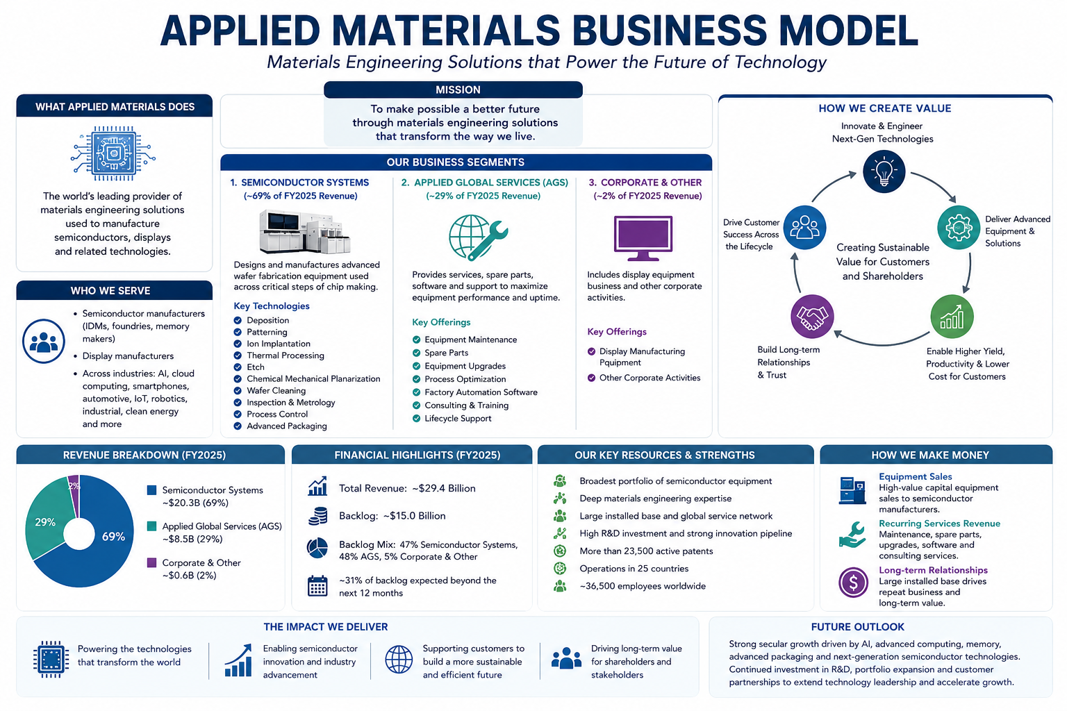
Applied Materials operates a technology-driven, vertically integrated business model centered on developing, manufacturing, and servicing advanced materials engineering solutions for the semiconductor industry. Rather than manufacturing semiconductors itself, the company supplies the equipment, software, and services that chipmakers use to produce increasingly sophisticated integrated circuits. Its business model combines high-value capital equipment sales with recurring service revenue, creating long-term customer relationships that extend throughout the lifecycle of semiconductor fabrication plants.
The company’s operations are organized into two primary business segments. The Semiconductor Systems segment designs and manufactures wafer fabrication equipment used across nearly every stage of semiconductor production, including deposition, ion implantation, chemical mechanical planarization (CMP), thermal processing, wafer cleaning, process diagnostics, inspection, metrology, and advanced packaging. Customers purchase these highly specialized systems to build and upgrade fabrication facilities capable of manufacturing advanced chips for AI, cloud computing, smartphones, automotive electronics, and other high-growth applications. As semiconductor technology evolves, customers continue investing in new equipment to improve performance, increase manufacturing yields, and support next-generation process technologies.
Complementing equipment sales is the Applied Global Services (AGS) segment, which generates recurring revenue by supporting the company’s large installed base of manufacturing systems worldwide. AGS provides spare parts, maintenance services, equipment upgrades, consulting, process optimization, and factory automation software that help customers maximize productivity, improve equipment uptime, and extend the operational life of fabrication tools. Because semiconductor manufacturing facilities operate continuously and require extremely high levels of precision and reliability, these lifecycle services create stable, long-term customer relationships while generating predictable recurring revenue.
Applied Materials invests heavily in research and development to maintain its technology leadership. The company works closely with leading semiconductor manufacturers to develop new materials engineering solutions for advanced logic, memory, and packaging technologies. This collaborative innovation model enables Applied Materials to introduce next-generation manufacturing equipment that supports evolving customer requirements while reinforcing long-term partnerships. By combining advanced equipment, lifecycle services, software, and continuous innovation, Applied Materials has built a scalable business model that benefits from both semiconductor capital investment cycles and recurring demand generated by its global installed base.
How Applied Materials Makes Money
Applied Materials generates revenue primarily by selling semiconductor manufacturing equipment and providing lifecycle services that help customers maximize the performance of their fabrication facilities. Its business is built on two complementary revenue streams: Semiconductor Systems, which supplies advanced wafer fabrication equipment, and Applied Global Services (AGS), which generates recurring revenue through maintenance, spare parts, software, upgrades, and consulting services. This combination enables the company to benefit from both new semiconductor capacity investments and the ongoing operation of customers’ existing manufacturing facilities.
The Semiconductor Systems segment is Applied Materials’ largest source of revenue. The company sells highly specialized equipment used for deposition, ion implantation, chemical mechanical planarization (CMP), thermal processing, wafer cleaning, inspection, metrology, process diagnostics, and advanced packaging. As semiconductor manufacturers invest in new fabrication plants and transition to smaller process nodes and AI-focused chip architectures, they purchase Applied Materials’ equipment to improve manufacturing precision, increase yields, and enable next-generation semiconductor production. In fiscal 2025, Semiconductor Systems generated approximately $20.3 billion, representing nearly 69% of the company’s total revenue.
The second major revenue stream comes from Applied Global Services (AGS). Once customers install manufacturing equipment, they require continuous support to maintain high levels of productivity and reliability. AGS provides spare parts, equipment upgrades, maintenance contracts, consulting, process optimization, and factory automation software that improve equipment utilization and extend the life of semiconductor manufacturing systems. Because semiconductor fabrication plants operate around the clock and equipment downtime is extremely costly, these services create recurring revenue and long-term customer relationships. In fiscal 2025, AGS generated approximately $8.5 billion, contributing around 29% of total company revenue.
The company also operates a smaller Corporate and Other segment, which includes display manufacturing equipment and generated approximately $607 million in revenue during fiscal 2025. Overall, Applied Materials reported total revenue of approximately $29.4 billion in fiscal 2025 while maintaining strong profitability driven by its diversified business model. The company also ended the year with a backlog of approximately $15.0 billion, providing strong visibility into future revenue. About 47% of the backlog was attributed to Semiconductor Systems, 48% to Applied Global Services, and the remaining 5% to Corporate and Other. Additionally, approximately 31% of the backlog is expected to be recognized beyond the next 12 months, reflecting sustained customer demand.
Applied Materials further strengthens its earnings through long-term relationships with leading semiconductor manufacturers. As customers build new fabrication facilities, expand AI chip production, and upgrade existing manufacturing lines, they continue purchasing new equipment while relying on AGS for ongoing maintenance and optimization. This combination of capital equipment sales, recurring service revenue, and a large installed base enables Applied Materials to generate stable cash flows while benefiting from long-term growth in semiconductor demand driven by artificial intelligence, cloud computing, advanced packaging, and next-generation electronics.
Future Outlook
Applied Materials expects long-term growth to be driven by structural trends reshaping the semiconductor industry, particularly the rapid adoption of artificial intelligence (AI), high-performance computing, advanced memory, and increasingly complex chip architectures. As semiconductor manufacturers transition to smaller process nodes, heterogeneous integration, and advanced packaging technologies, the need for innovative materials engineering solutions is expected to increase. The company believes these technology shifts will create significant opportunities across its semiconductor equipment portfolio, especially in areas such as patterning, process control, packaging, and materials innovation.
To capitalize on these trends, Applied Materials plans to continue investing heavily in research and development while working closely with customers to develop next-generation manufacturing technologies. The company also expects its large installed base to support continued growth in Applied Global Services through equipment upgrades, software, maintenance, and optimization services. By combining technology leadership, a broad product portfolio, and deep expertise in materials engineering, Applied Materials aims to strengthen its position as a critical partner to semiconductor manufacturers as AI, cloud computing, automotive electronics, and other advanced technologies continue to drive demand for increasingly sophisticated semiconductor devices.